this post was submitted on 23 Nov 2024
56 points (96.7% liked)
Electronics
2230 readers
1 users here now
Projects, pictures, industry discussions and news about electronic engineering & component-level electronic circuits.
Rules
1: Be nice.
2: Be on-topic (eg: Electronic, not electrical).
3: No commercial stuff, buying, selling or valuations.
4: No circuit design or repair, tools or component questions.
5: No excessively promoting your own sites, social media, videos etc.
Ask questions in https://discuss.tchncs.de/c/askelectronics
founded 2 years ago
MODERATORS
you are viewing a single comment's thread
view the rest of the comments
view the rest of the comments
What are double sided breadboards?
Perfboards?
These can be double sided and can be soldered to.
Breadboads can only be one sided.
Edit: this is a solderless breadboard. Non-solderless breadboards do exist, as I learned today.
Thank you! I thought I was losing my mind.
Probably double-sided prototyping PCBs. The double-sided ones tend to be green (FR4 fiberglass resin), the single-sided orange (FR2 paper phenolic-resin).
Terminology varies, a lot of greymarket sellers use "veroboard", "prototype board" and "breadboard" interchangeably.
The glue between the copper pads and the board itself tend to better with the double-sided boards, I agree with you OP :) Although this isn't universal, I've had some nasty bare copper boards on FR4 where the pads pop off when you try to solder to them; and some old FR2 boards with really well adhered pads. I've read somewhere that this might (?) be due to moisture in the PCB boiling off when you put the soldering iron to a pad and that baking the board in an oven first can help, but I have not tried that. I suspect a lot of it comes down to the quality of adhesive used between copper and substrate.
They're pretty much the same as a solderless breadboard, in that they have dedicated power/signal rails and multiple rows/groups of bridged pads. They are usually used for a working prototype, as opposed the solderless ones used for initial circuit design/debug on a benchtop.
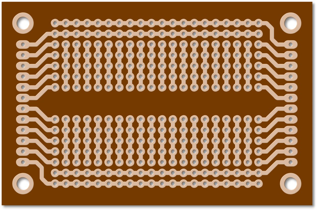
Here's a general design with dedicated in/output pads.
Presumably prototyping boards with plated thru holes.
Both sides have copper plating to wet solder to.